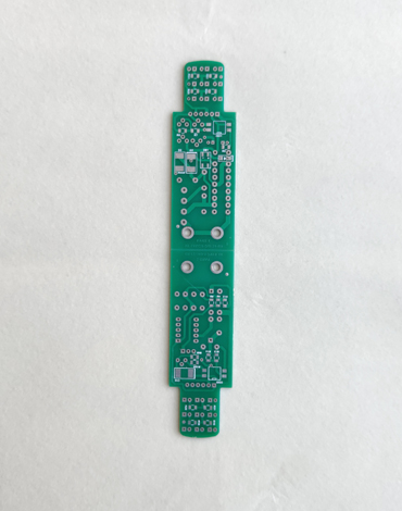
Double Sided PCBs

Double Sided PCBs
When it comes to printed circuit boards, double sided PCBs are a common option in the market because they enable more complicated designs, circuits, and consequently advantages for products. Contrary to single sided PCBs, the conductive copper and components can be mounted on both sides of the board instead of just one.
Due to the ability to alternate between the top and bottom layers via vias, these double-sided boards enable closer routing traces. As a result of holes being drilled into the board, the circuits on one side of the board can be connected to those on the other, which can be highly beneficial in many electrical goods.
It is known as a double-sided PCB or two-layer PCB because there are two or double conductive layers that make up the circuit. These circuit boards support connections between components utilising two practical technologies: through hole technology and surface mount technology. Both technologies have advantages and disadvantages depending on your demands and requirements. Double sided PCBs are frequently used in electrical industry for circuits ranging from simple to complicated.
Double-sided PCBs have many benefits to them. From higher flexibility to a greater density of circuits, Double-sided PCBs offer maximum utilization of space, because the components can be placed on both the sides of the board. It is cost-effective, comes in a compact size, and can be used for projects that need to be intricately designed.
