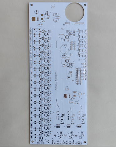
Multi-layer PCBs

Multi-layer PCBs
All multilayer PCBs are required to have at least three layers of conductive material buried in the middle, as opposed to the two conductive layers that are present on a double-sided PCB. Multilayer PCBs are made by laminating alternating layers of prepeg and core materials together at high temperatures and pressure.
This procedure makes sure that the layers are correctly melted and cured, that the conductors are entirely enclosed by resin, and that there is no trapped air between the layers. The variety of material combinations is wide, ranging from straightforward epoxy glass to unusual ceramic or Teflon components.
Prepeg and core are essentially the same material, although prepeg is more pliable than core since it has not entirely dried. The layers are then put into a laminating press in alternate directions. The stack up is subjected to extremely high pressures and temperatures, which causes the prepeg to "melt" and fuse the layers together. The finished product is a multilayer board that is highly sturdy and durable after cooling.
Consumer electronics, telecommunications, defence and military, among other industries, use multilayer PCBs, which are ordinary electrical boards made up of two or more inner layers. They have a compact design, numerous functionalities, lightweight production, durability, and flexibility.
A PCB board substrate that has been properly constructed can effectively lower crosstalk and electromagnetic emissions while also enhancing signal integrity to deliver low inductance power. Instead of trying to eradicate the noise after the product has been made, the external noise needs to be muffled at the source. When compared to double-sided boards, the right design of multilayer PCBs can boost immunity to RF fields by a factor of 10 or more. Yet overall, compared to any other straightforward double-sided printed circuit board, multilayer boards are more expensive and challenging to troubleshoot. Yet, there are more layout alternatives for this type of board design and multilayer PCBs provide superior shielding and signal routing. Compared to single- or double-sided boards, multilayer PCBs offer more density for power and data routing.
Products like computers, file servers, X-Ray equipment, atomic eaccelerators, Industrial controls, satellite systems and many more complex devices use multi-layer PCBs.
